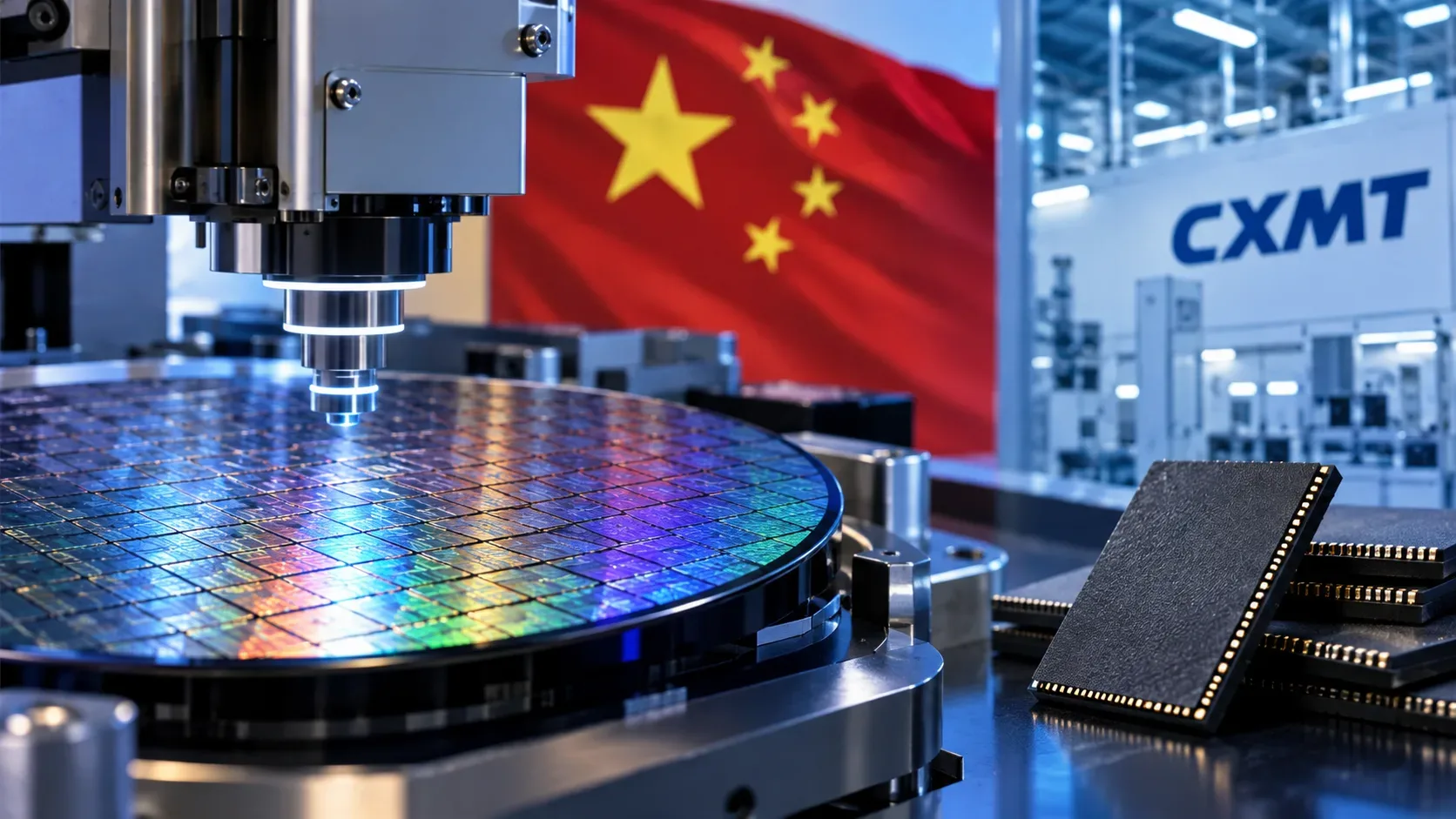
China's ChangXin Memory Technologies, or CXMT, announced on September 20, 2026 that its fifth-generation DRAM platform, called G5, had entered mass production. The announcement matters because it combines a reported reduction in the spacing of critical memory structures, new 24-gigabit LPDDR5X chips, and an increase of at least 50% in the gross number of dies that can be formed per wafer compared with the previous generation, using an 8 Gb baseline.
The key point, however, is to separate industrial progress from proven leadership. The disclosed figures show process progress and higher potential density, but they do not by themselves provide final manufacturing yield, actual monthly output, or a direct equivalence with the commercial node labels used by Samsung, SK hynix and Micron. The safer reading is that CXMT has narrowed part of the technology gap and expanded its ability to compete, especially inside China's ecosystem, without the announcement proving global industry dominance.
What CXMT announced
According to Reuters, CXMT said G5 is already in mass production. The company presented the platform at the 2026 World Manufacturing Convention in Hefei and said it was designed to deliver more memory capacity per chip, lower power consumption and better cost efficiency.
- Platform: fifth-generation DRAM, or G5.
- Disclosed scale: 11.95 nm spacing in a critical structure of the memory array's active area.
- Technique: quadruple patterning, a multi-step process used to create finer patterns.
- Products introduced: two 24 Gb LPDDR5X versions aimed at smartphones and other portable devices.
- Product density: 24 Gb per die, 50% more data than the company's previous comparable 16 Gb products.
- Per-wafer gain: at least 50% more gross dies per wafer than the fourth-generation platform, according to CXMT, based on an 8 Gb chip comparison.
Reuters also reported that CXMT attributes the platform's development to computer simulations and joint work with Chinese equipment suppliers on critical production steps.
What 11.95 nm and quadruple patterning mean
The 11.95 nm figure should not automatically be read as a node name equivalent to the commercial labels used by other manufacturers. It refers to the spacing of a specific structure in the data-storing area. Direct comparisons between that figure and terms such as “12 nm class” require caution because each manufacturer can use different metrics and naming conventions.
Quadruple patterning makes it possible to create smaller structures by combining lithography with additional deposition and etch steps. imec describes self-aligned quadruple patterning as a technique in which an initial pattern is multiplied through spacers, increasing line density. ASML explains that multipatterning extended the capabilities of immersion lithography, although at the cost of greater process complexity and strict requirements for overlay control and productivity.
For CXMT, bringing this kind of process into mass production matters because memory manufacturing depends not only on designing smaller structures, but on reproducing them at high volume with tight control over variation, defects and cost.
The 50% per-wafer gain is not the same as yield
This is the most important caveat in reading the announcement. CXMT said G5 can produce at least 50% more gross dies per wafer than its fourth-generation platform, using 8 Gb chips as the comparison baseline. Gross dies are the units that physically fit on the wafer before defective units are removed.
Yield measures the share of dies that pass testing and can be sold. More gross dies per wafer can reduce the potential cost per chip, but it does not reveal on its own how many saleable chips come from each wafer. The company also did not provide, in the cited announcement, a yield rate or a specific monthly output figure for G5.
That does not negate the advance. It simply limits what can be concluded. To measure industrial competitiveness, observers will need to watch sustained production, quality stability, customer adoption and costs over the coming quarters.
Where CXMT stands in the DRAM market
The company remains behind the three global leaders, but it already holds a material position. Data from TrendForce indicates that CXMT's share of global DRAM revenue rose from 7.6% in the first quarter of 2026 to 9.5% in the second quarter. Over the same period, Samsung held 39.4%, SK hynix 24.9% and Micron 23.3%.
The market context also matters. TrendForce says global DRAM industry revenue increased 59.5% in the second quarter of 2026, driven by higher prices and demand tied to AI servers, HBM, LPDDR5X and high-capacity modules. In other words, CXMT is expanding in a strong market with intense competition for capacity.
G5 may strengthen the company in mobile memory and higher-density products, but revenue share alone is not a measure of technology leadership. Product mix, manufacturing yield, scale in server memory and presence in HBM remain important variables when comparing suppliers.
Why the advance has strategic weight for China
The announcement connects to China's effort to reduce external dependence on critical components and equipment. Since 2022, the United States has expanded controls on exports to China of certain advanced semiconductor manufacturing technologies. In December 2024, the Bureau of Industry and Security announced additional restrictions covering more types of manufacturing equipment, software and high-bandwidth memory.
In that environment, a denser platform developed with participation from Chinese equipment suppliers has value beyond the finished chip. It can build experience in equipment, materials, metrology, process control and integration, the areas that determine the resilience of a semiconductor supply chain.
At the same time, technological sovereignty does not mean complete self-sufficiency. Memory fabs depend on an international network of machines, materials, intellectual property, software and specialized suppliers. G5 matters because it expands the share China can execute domestically and can reduce some bottlenecks, not because it proves that all external dependencies have disappeared.
What the announcement still does not prove
| What is confirmed | What still needs additional evidence |
|---|---|
| CXMT says G5 is in mass production. | Final yield of the new platform at commercial scale. |
| The company disclosed 11.95 nm for a critical structure in the active area. | Direct equivalence with competitors' process naming. |
| Two 24 Gb LPDDR5X products were presented as being in mass production. | Monthly shipment volume and breadth of customers. |
| CXMT claims at least 50% more gross dies per wafer than G4. | Effective cost per bit after defects, testing and packaging. |
| The company held 9.5% of global DRAM revenue in Q2 2026, according to TrendForce. | Its ability to sustain market-share gains in less favorable pricing cycles. |
What to watch next
The most useful next signals will be operational rather than promotional: customer products using the new chips, the evolution of the LPDDR5X and DDR5 mix, recurring production data, any yield disclosures, capacity expansion, and progress in server memory and HBM.
It will also be important to see whether the higher density per wafer translates into more competitive prices without sacrificing margins, and whether Chinese equipment suppliers can sustain a role in critical process steps. Those factors will say more about industrial sovereignty than a single geometry metric.
In short, G5 mass production is a meaningful milestone for CXMT and for China's memory strategy. It shows a combination of growing scale, a denser process and a broader product portfolio. What remains to be demonstrated is how far those gains translate into yield, cost, volume and sustained competitiveness against the global leaders.